Bielefeld: Prof. G. Reiss Mainz: Prof. M. Kläui ► Contact

Welcome to ForLab MagSens: Center of Competence for high performance magnetic sensor systems!

ForLab MagSens is a joint center of Bielefeld University and Johannes Gutenberg-University Mainz.
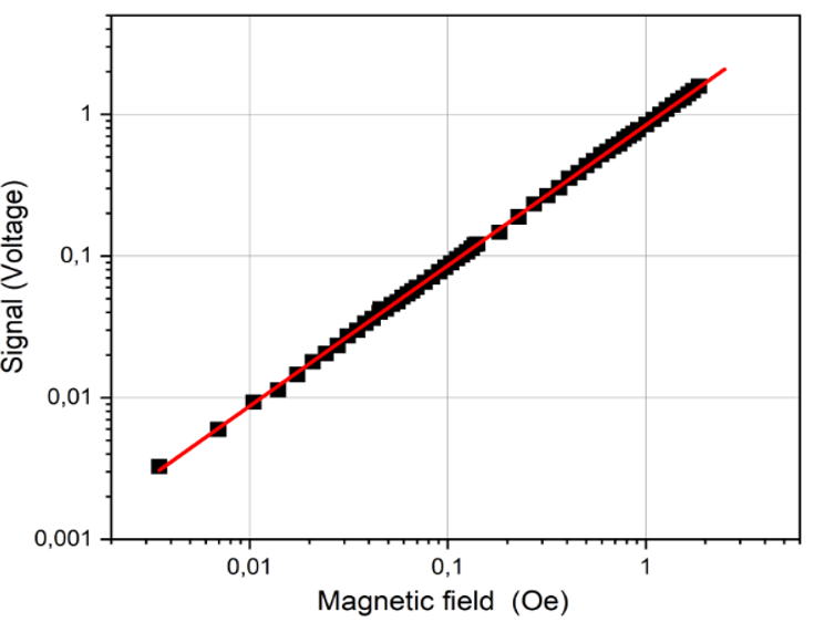
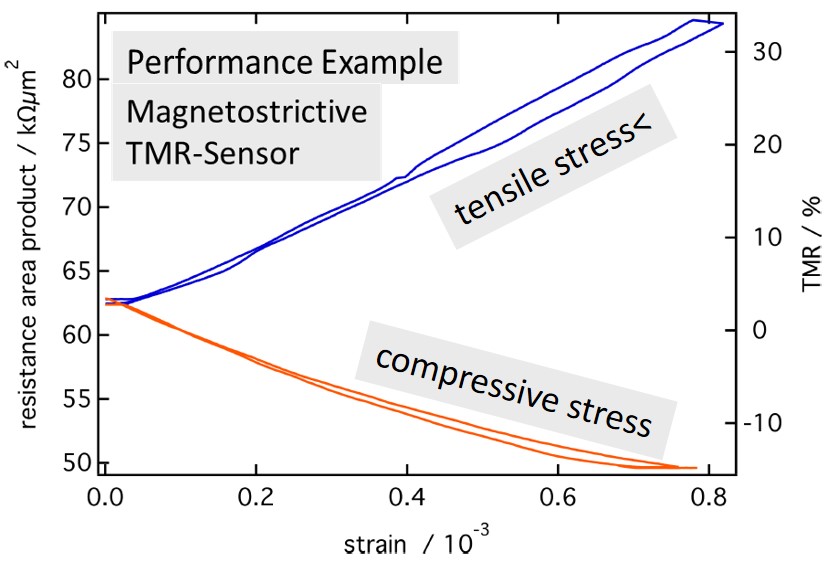
We are dedicated to research for and development of new magnetic sensor systems that can measure position and angle of moving parts, mechanical stress and many other quantities you want to detect. We offer an exceptional and stimulating research environment for tailoring the sensing systems to meet the requirements of magnetic sensors' applications in automatisation, automotive, Industry 4.0 or biotechnology.

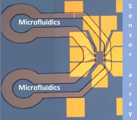
  • pools the complete scientific and technical Know-How on the design, development and realization of magnetic stand-alone sensors and complete sensor systems.
  • offers support and collaborations to create adapted high performance magnetic sensor systems for detection of position, angle, magnetic field or other quantities in applications such as automatisation, automotive, compasses, material inspection and similar.
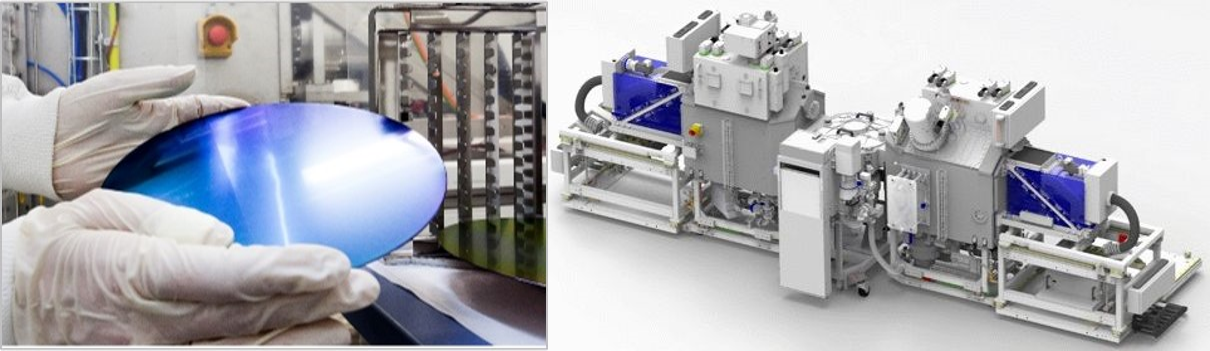
  • covers the R & D requirements from the integration of new materials in thin film stacks for magnetic sensors, the analysis and optimization of the sensing performance up to 8-inch wafer scale coating and lithography for demonstrators.

News

  • Workshop: Magnetic Sensing & Spintronics (within symposium „Mikroelektronik Forschung in Deutschland: von den Grundlagen zur Anwendung“)
    • Date: 30.3.2022, 14.00
    • Venue: Online
Magnetoresistive effects are already widely exploited in magnetic sensors and in magnetic memories. New developments exploit the spin orbit effects in heavy metals and at interfaces between materials to manipulate or sense the magnetic state with the aim to either enhance the sensitivity or endurance or to induce new functionalities as reconfigurable logic functions. The workshop aims to bring together experts from industry and research institutes and to show exemplarily the importance of this field for the microelectronics in Germany. The link for online participation will be mailed to registered participants.
Speakers: W. Raberg, Infineon; A. Kehlberger, Sensitec; O. Matthes, Fraunhofer ENAS; G. Reiss, Bielefeld University.

Participation is free! Please use the following links:
• Registration at VDI-VDE (required).     • Workshop flyer.     • Contact coordinator G. Jakob, Mainz.


Wafer
8 inch wafer coating
Sensing technologies:

We use state-of-the-art thin film stacks for realizing sensing systems that are based on:

► Giant
MagnetoResistance (GMR)
► Tunneling
MagnetoResistance (TMR)
► Anisotropic
MagnetoResistance (AMR)
► Planar
Hall Effect (PHE)

Major equipment:
  • Ultrahigh Vacuum Sputtering:: Wafer size up to 8". Up to 16 sputter sources. Smooth and homogeneous thin film systems. Metals and insulators. Co-deposition for combinatorial materials research

  • Molecular Beam Epitaxy: Single crystalline thin film systems. Wafer size up to 4". Up to 8 MBE sources. Metals and insulators. Co-deposition for combinatorial materials research

  • Atomic layer deposition: Up to 4" sample size. Aluminum-Oxide films. Reliable insulation down to 5nm film thickness. Conform film growth also on 3-d shaped samples.

  • Transport Characterization: Resistance, Magneto- and Tunneling-Magnetoresistance, Hall-Effects. Seebeck- and Nernst-Effects. Temperatures from 1.5K to 500°C. Dc and ac-techniques including Lock-In

  • Structural and composition analysis: Scanning- and Transmission Electron microscopy. Atomic Force microscopy. X-ray diffraction and -reflection. Resonant X-ray diffraction and -reflection at synchrotrons. Energy Dispersive X-ray Analysis. X-ray Fluorescence. Scanning Auger Microscopy with depth profiling.

  • Lithographic processing: Optical and e-beam lithography. Up to 8" (optical) / 4" (e-beam). Three metallization levels. Patterning of tunneling devices. Ion beam etching and reactive etching with stop-control. Mask preparation. Clean room environment.
Mikrofl2
Sensor array integrated in microfluidics

TMRs
TMR-Sensors for mOe-detection

TMRs
TMR-Sensors for mechanical stress detection